Archive for July 31, 2012

Metamaterials Entering The Commercial Market as Miniaturized Antennas

Image

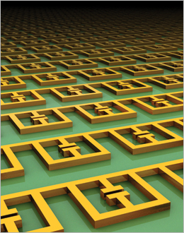
Metamaterials are a very interesting advanced material.  Metamaterial can be described as an electromagnetic composite in which structure and constituent materials determine how it will affect the propagation of light.  Metamaterials typically include several classes of electromagnetic composites including photonic crystals, negative index materials, low index materials, zero index materials, and  chiral metamaterials.  The wavelength or frequency at which they control the propagation of light and therefore energy is a function of the size of the periodic  features.  For photonic crystals, the feature is on the order of the wavelength of light.  For the other classes of metamaterials, the feature size can be 10 times to 100 times smaller than the wavelength of light.  In the age of smart phones, in which multi-band operation, lighter and lower profile products are desired by users, metamaterials have finally found a home in the world of mobile phone antennas.

Rayspan has successfully commercialize metamaterials by integrating them into antenna applications.  Netgear became Rayspan’s first customer.  To date, Rayspan has shipped over 25 million metamaterial antennas in routers.  LG was the next customer.  LG has integrated Rayspan’s low profile, multi-band metamaterial based antenna into the LG Chocolate smart phone.   LG’s president notes that this enabled them to achieve a much sleeker product with improved antenna performance.  Since, Rayspan has signed a licensing agreement with another undisclosed mobile phone provider.  Rayspan’s success at commercializing a metamaterials based product is notable.

Since the discovery of metamaterials by Marconi in 1919, these advanced materials have not successfully penetrated the commercial market.  Frost & Sullivan note that successful integration and commercialization of metamaterials into applications has been plagued by:

  • lack of customer awareness
  • technical difficulties in design and fabrication
  • loss (absorption in metamaterials)
  • lack of collaborative efforts

I led a research program at a large aerospace company for five years in the area of metamaterials.  Based on my own experience, I would say that the lack of customer awareness (and customer pull) was the biggest problem.  The next challenge was to appropriately match the class of metamaterial to a targeted application area.  I took into account the maturity of metamaterial fabrication and design and the absorption of the metamaterial and the constituent materials.  Finally, the metamaterial would need to be matched to the appropriate application.  Specifically, the integration of the metamaterial would need to enhance various desired performance characteristics one to two orders of magnitude.

Metamaterials have the potential to transform the current technology landscape in several industries.  Future posts will discuss advances in the design, fabrication and integration of metamaterials into applications.

Aerographite is a Breakthrough in Light Weight and Multifunctional Materials

In the past few months, a new material has come into light – aerographite.

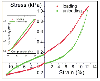
It has several remarkable properties.  The most noteworthy is its low density.  It has the lowest density of any material ever created including air.  The density is 0.2mg/cm3.  In addition, it can be compressed three orders of magnitude and then spring back to its original size.  It is also electrically conductive and conductivity can be modified by compressing the material. [1]

Image

The structure is an interconnected network of closed shelled microtubes.  The walls of these tubes are approximately 15 nanometers thick but have a tube diameter in the order of a micron or more.  Unlike multiwalled carbon nanotubes, the microtubes show less curvature.  The tube surface can be modified by growth conditions to introduce wrinkles that increase mechanical stability.

It is processed from ZnO powder that is heated to 900°C.  This transforms the ZnO to a three dimensional network of nanocrystals and microcrystals.  This is then placed into a chemical vapor deposition reactor where carbon and hydrogen rich gas sources are introduced at a chamber temperature of 760°C.  Aerographite can currently be fabricated up to a volume of several cubic centimeters.

Other interesting properties include:

  • high optical absorption.  It appears black
  • flexible and compressible.
  • hydophobic so will wet well to epoxies.
  • high temperature stability
  • chemically resistant

Some potential applications include:

  • Electronics for aerospace applications.  The low density property means low acceleration forces which is ideal for high impact and high vibration environments.
  • Electrode for Li ion batteries.  Mechanical robustness, high surface area and low specific weight are all beneficial properties for this application.

Reference:

[1]  http://onlinelibrary.wiley.com/doi/10.1002/adma.201200491/pdf

Graphene is an Advanced Material to Keep an Eye On

Graphene is one of a handful of advanced materials that when successfully manufactured on a large scale and integrated will transform many areas of industry including (but not limited to) electronics, construction, and optics over the next several decades.

Graphene is a single-atom thick sheet of sp2-bonded carbon atoms that make up a hexagonally closed packed two-dimensional lattice.  From this description, it is clear to see that this material offers a very high surface to volume ratio.  It will have very different in-plane properties compared to out of plane properties.  It is easy to guess it is very strong (in-plane tensile strength is 200 times that of steel).  It is basically an unzipped carbon nanotube.

Image

Graphene is a material with a unique combination of properties.  These include electrical properties such as high electron mobility (15,000cm2V-1s-1) which is nearly temperature independent from 10K to 100K.  It has a sheet resistivity that is less than silver (10-6W) and yet is still transparent at visible wavelengths.  Optical properties include a voltage tunable band gap and the nonlinear Kerr effect.  Notable thermal properties include an in-plane conductivity similar to diamond (1000W/mK).  Mechanical properties include a tensile modulus of 1TPa.  It can also be stretched at 20% of its length and still maintain structural integrity.

This remarkable material has attracted much interest in both research and commercial sectors.  Currently, over 200 small and medium sized companies are working on the manufacturing of graphene (both bottom-up and top-down approaches) and its integration into products.  A few applications of interest include:

  • flexible electronics
  • conductive inks
  • super lubricant
  • hydrophobic coatings
  • high frequency integrated circuits

According to a Frost and Sullivan March 2012 report titled “Advances in Graphene Technologies – Emerging Business Opportunities”, manufacturing of large sheets of high quality graphene is a key bottle neck for its integration into the electronics industry.  They estimate that this should be achieved in four years (if not sooner).

Collaborative efforts between companies and academia have developed and are seen as key in making progress in manufacturing challenges.  These include the Graphene Flagship and the Korean Graphene Hub.

It is estimated that graphene-enhanced products will be the first to reach the market and that graphene-enabled products will follow about a decade later.